In the case of low-energy electron diffraction (LEED) investigations, the solid surface is irradiated with low-energy electrons. The resulting diffraction pattern, which can be viewed on a screen, permits statements about the structure of the surface. Low-energy electrons (30-300 eV) have wavelengths of the order of the interatomic distances (de Broglie equation: l = h / p), both parallel and perpendicular to the solid surface. As a result, the electrons can be elastically scattered from the surface atoms of the solid body. Since the scattering cross-section is very large for low-energy electrons, the penetration depth of the electron beam is in the range of a few atomic layers. The diffracted electrons fly radially away from the sample to a screen, where they are made visible as fluorescent spots. This diffraction pattern is an image of the reciprocal lattice of the solid surface, and information about the symmetry, size of the surface unit cell, and the quality (purity) of the surface can be obtained.

LEED image of a pure W (110) surface with an e energy of 138eV
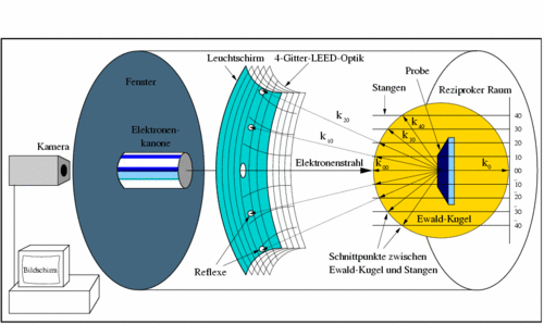
Schematic structure of a LEED optics